LPDDR6 Explained: Speed, Release Date and LPDDR6 vs LPDDR5X
JEDEC finalized LPDDR6 in July 2025. Here is what SK hynix and Samsung have actually confirmed about speed, power efficiency, and when it reaches phones.
LPDDR6 is the next mobile memory standard, finalized by JEDEC as JESD209-6 in July 2025. It is a mobile-only successor to LPDDR5X, not the same thing as desktop DDR6 or GDDR7, and it is not in any shipping phone yet. SK hynix and Samsung have each announced their own early LPDDR6 chips reaching roughly 10.7 Gbps per pin, with SK hynix separately claiming the architecture is about 33% faster and more than 20% more power-efficient than LPDDR5X. Both companies are targeting mass production in the second half of 2026, which means phone-ready LPDDR6 realistically lands in flagship devices sometime in 2026 or 2027, not this holiday season.
- What it is: JEDEC's JESD209-6 standard, the sixth generation of Low-Power DDR memory built for phones, tablets and other battery-powered devices.
- Finalized: July 9, 2025, by the JEDEC Solid State Technology Association.
- Speed: SK hynix's March 2026 chip and Samsung's CES 2026 chip both start at roughly 10.7 Gbps per pin; the standard itself allows for higher grades up to 14.4 Gbps as the ecosystem matures.
- Efficiency: SK hynix claims over 20% lower power use versus LPDDR5X; Samsung claims about 21% greater energy efficiency versus its previous generation.
- Timeline: Both vendors are targeting mass production in the second half of 2026; phones with LPDDR6 are not confirmed yet.
What Is LPDDR6?
LPDDR6 (Low-Power Double Data Rate 6) is a memory standard built specifically for devices where battery life and heat matter as much as raw speed: smartphones, tablets, laptops and increasingly on-device AI accelerators. It is the direct successor to LPDDR5X, which has shipped in flagship phones for several years, and it is defined and ratified by JEDEC, the same standards body that governs desktop DDR, GDDR graphics memory and HBM.
It is important to separate LPDDR6 from two other memory families this site has already covered. It is not desktop DDR6, which is a separate, still-unfinished standard aimed at PCs and servers and governed by its own JEDEC working group (more on that distinction below). It is also not GDDR7, the graphics-card memory standard explained in our GDDR7 explainer, which trades power efficiency for sheer bandwidth on dedicated graphics cards. LPDDR6 occupies its own lane: mobile-first, power-constrained, soldered directly onto a phone or tablet's logic board rather than socketed or swappable, continuing a lineage that traces back through earlier LPDDR generations.
The JEDEC JESD209-6 Standard, Explained
JEDEC, the Solid State Technology Association that standardizes memory for the entire industry, published JESD209-6 on July 9, 2025. That publication is what most outlets mean when they say "LPDDR6 was finalized" — it is the formal specification, listed on JEDEC's own standards page, that chipmakers like SK hynix, Samsung and Micron design their actual silicon against, the same way JESD79 governs desktop DDR generations.
Industry coverage of the standard describes a few structural changes from LPDDR5X. LPDDR6 moves to a 24-bit channel built from two independent 12-bit sub-channels, rather than LPDDR5X's wider single-channel approach, which JEDEC and early analysis describe as roughly doubling effective bandwidth per channel at a given clock. The standard also widens on-die reliability features, adding expanded on-die ECC, parity checking and self-test capability, and it covers device densities from 4Gb up to 64Gb per die, giving chipmakers room to scale capacity well past today's flagship phone configurations.
Full access to the JESD209-6 document itself is paywalled for non-JEDEC members, which is normal for JEDEC specs and part of why so much of the public detail comes through chipmaker announcements rather than the standard's text directly.
LPDDR6 vs LPDDR5X: What Actually Changes
The headline framing from both SK hynix and Samsung is "faster and more efficient than LPDDR5X," but the two vendors are not describing identical products, and neither company has shipped a phone-ready part yet. Here is how the standard-level architecture compares, separate from either company's specific chip:
| Spec | LPDDR5X | LPDDR6 |
|---|---|---|
| JEDEC standard | JESD209-5 | JESD209-6 |
| Finalized | 2021 (with later extensions) | July 2025 |
| Channel architecture | Single wide channel (x16/x32) | 24-bit channel split into two independent 12-bit sub-channels |
| JEDEC data rate ceiling | Up to ~8.5 Gbps per pin at standard; vendors have since pushed proprietary variants higher | Specified up to roughly 14.4 Gbps per pin |
| On-die reliability | Basic on-die ECC | Expanded on-die ECC, parity and self-test |
| Device density | Up to 32Gb per die | 4Gb to 64Gb per die |
In practice, the first real LPDDR6 chips from SK hynix and Samsung both start around 10.7 Gbps per pin, which is close to the fastest proprietary LPDDR5X variants some vendors have already shipped. That is not a contradiction: JEDEC's 14.4 Gbps figure is the ceiling the standard supports, not the speed of any chip announced so far. The actual generational gain, according to the vendors themselves, is less about peak per-pin speed on day one and more about architecture — the sub-channel split, reliability features and power-management logic that let LPDDR6 do more work per watt than LPDDR5X at a similar clock.
SK hynix's LPDDR6 Figures
SK hynix announced its first LPDDR6 milestone in a March 2026 newsroom post: a 16Gb LPDDR6 die built on the company's "1c" process, its sixth-generation 10-nanometer-class node. According to SK hynix's own announcement, the chip's base operating speed exceeds 10.7 Gbps per pin, which the company says is faster than the top speed of existing mass-produced memory. SK hynix attributes a 33% increase in effective data processing speed to the new architecture's expanded bandwidth, and says it cut power consumption by more than 20% compared with the previous generation through a sub-channel structure combined with dynamic voltage and frequency scaling (DVFS).
SK hynix is targeting smartphones and tablets running on-device AI as the primary market, and specifically calls out high-spec mobile gaming as a workload that benefits from the chip's higher DVFS levels. The company says it finished validating its 1c LPDDR6 development after first showing the chip at CES 2026, with mass-production preparation wrapping up in the first half of 2026 and actual supply beginning in the second half of the year.
Samsung's LPDDR6 Figures
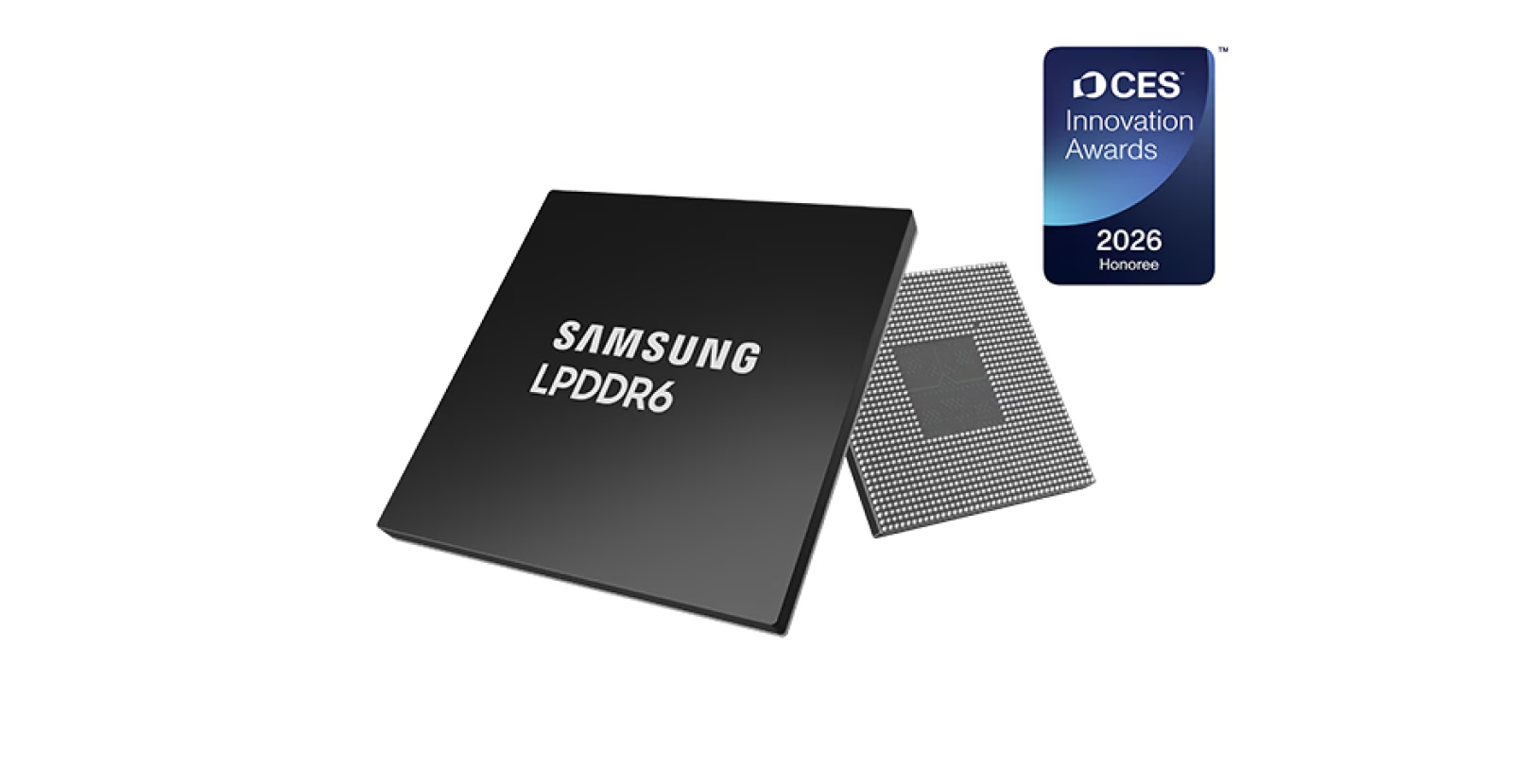
Samsung took its own first public LPDDR6 bow at CES 2026, where the chip was named a CES Innovation Awards 2026 honoree in the Mobile Devices, Accessories and Apps category. According to Samsung's own semiconductor newsroom, its LPDDR6 reaches data rates of up to 10.7 Gbps with an expanded I/O count to maximize bandwidth, scales up to 16GB of capacity, and delivers roughly 21% greater energy efficiency than its previous generation. Samsung credits the gain to a combination of enhanced DVFS, a new "Dynamic Efficiency Mode," a proprietary Smart PMIC, and circuit changes that widen the chip's low-power operating range.
Samsung also emphasizes hardware-based security additions covering data integrity, authentication, device-level and system-level protection — features aimed as much at automotive and enterprise AI servers as at phones. The company describes itself as first to bring a JESD209-6-based product to market, though its newsroom material does not commit to a specific consumer launch date or a confirmed phone design win.
Because SK hynix and Samsung are reporting different things — SK hynix a specific 16Gb die with a stated 33%/20% improvement pair, Samsung a broader LPDDR6 platform with a 21% efficiency claim — it's worth keeping the two separate rather than averaging them into one number. Here's how the public claims line up side by side:
| SK hynix | Samsung | |
|---|---|---|
| Announced | March 2026 (development completed) | CES 2026 / January 2026 |
| Speed | Base speed over 10.7 Gbps per pin | Up to 10.7 Gbps per pin |
| Process | "1c," 6th-generation 10nm-class | Not disclosed |
| Capacity shown | 16Gb die | Up to 16GB module |
| vs. LPDDR5X | ~33% faster data processing; 20%+ less power | ~21% greater energy efficiency |
| Mass production target | 2H 2026 | Not specified; CES 2026 Innovation Award honoree |
LPDDR6 vs Desktop DDR6: Two Completely Different Standards
It's an easy mix-up because the names are one digit apart, but LPDDR6 and desktop DDR6 are separate JEDEC specifications developed on different timelines for different purposes. LPDDR6 (JESD209-6) is finished and already shown in silicon by two major DRAM makers; DDR6 for PCs and servers is still working through JEDEC's process and, as covered in our DDR6 RAM explainer, is not expected to arrive in consumer desktops for a while yet. The two standards also optimize for different things: desktop DDR prioritizes raw bandwidth and capacity per DIMM for a system that's plugged into a wall, while LPDDR6 prioritizes performance-per-watt for a device running on a battery with no active cooling. They are not interchangeable, not pin-compatible, and not on the same release schedule.
The same logic applies to graphics memory. GDDR7, which we cover separately, is built for the sustained, extreme bandwidth a discrete GPU needs and accepts much higher power draw to get it. LPDDR6 sits at the opposite end of that spectrum: it is designed to sip power while still keeping pace with on-device AI models and increasingly demanding mobile games.
Why Power Efficiency Is the Real Headline
For a desktop or graphics memory standard, the pitch is almost always "faster." For LPDDR6, both SK hynix and Samsung lead with efficiency because that's what actually matters inside a phone. A 20%+ reduction in memory power draw, as SK hynix claims, translates into either longer battery life at the same performance or more sustained performance before a phone has to throttle — which is exactly the trade-off that matters as on-device AI features push more inference workloads directly onto phone hardware instead of the cloud. Samsung's framing is similar: its Dynamic Efficiency Mode and expanded DVFS range exist specifically to let the chip idle down aggressively between bursts of AI or gaming workload, rather than running at a fixed high-power state.
This is also where the "33% faster" and "21% more efficient" figures can get flattened into a single marketing-style claim if you're not careful. SK hynix's 33% figure describes data-processing throughput gains from the new sub-channel architecture; its 20%+ figure describes power savings from the same architecture plus DVFS. Samsung's 21% figure describes power efficiency specifically, not speed. None of these numbers should be blended into a single "LPDDR6 is X% better" statistic, because they come from different companies, different test conditions, and in some cases different things being measured.
LPDDR6 Release Date: When It Actually Shows Up in Phones
As of this writing, LPDDR6 is not in any shipping phone. Both SK hynix and Samsung have said they are targeting mass production of their respective LPDDR6 chips in the second half of 2026. Mass production of a memory chip and that chip showing up in a phone you can buy are two different milestones, usually separated by a validation and qualification window with phone and chipset makers — the same gap that happened with LPDDR5X before it. Historically, that gap has run anywhere from several months to closer to a year.
That puts a realistic floor on phone-ready LPDDR6 somewhere in late 2026 at the earliest, with broader adoption more plausible through 2027 as more phone SoCs add LPDDR6 memory controllers and more fabs ramp up supply. Neither SK hynix's nor Samsung's own newsroom material commits to a specific phone or launch date, so any claim naming a specific upcoming flagship as the first LPDDR6 phone should be treated as speculation until the phone maker or the memory maker confirms it directly.
For anyone currently shopping and wondering whether to wait, our 2026 RAM buying guide is a better starting point than holding out for LPDDR6 — today's LPDDR5X phones are not about to become obsolete, and LPDDR6 handsets are not confirmed for this year.
What to Watch Next
A few concrete things will mark real progress between now and a retail LPDDR6 phone: either company confirming a specific mobile SoC partner that supports LPDDR6 memory controllers, either company publishing final JEDEC-certified speed grades rather than development-stage figures, and the first phone maker naming LPDDR6 in an actual product spec sheet rather than a press teaser. Until one of those happens, treat every "LPDDR6 phones in 2026" headline, including figures in this article, as a vendor roadmap target rather than a confirmed release date.
Frequently asked questions
What is LPDDR6?
LPDDR6 is the sixth-generation Low-Power DDR memory standard, finalized by JEDEC as JESD209-6 in July 2025. It is the mobile-specific successor to LPDDR5X, built for phones, tablets and other battery-powered devices rather than desktop PCs or graphics cards.
When will LPDDR6 phones be available?
No phone with LPDDR6 is confirmed yet. SK hynix and Samsung have both targeted mass production of their LPDDR6 chips for the second half of 2026, and phones typically follow mass production by several months to about a year.
How much faster is LPDDR6 than LPDDR5X?
It depends on whose figures you use. SK hynix says its LPDDR6 chip is about 33% faster at data processing than LPDDR5X, while Samsung's LPDDR6 announcement leads with a roughly 21% energy-efficiency gain rather than a speed claim. These are separate company-specific figures and should not be combined into one statistic.
Is LPDDR6 the same as desktop DDR6?
No. LPDDR6 and DDR6 are separate JEDEC standards on different schedules. LPDDR6 (JESD209-6) is finished and already shown in silicon by SK hynix and Samsung; DDR6 for desktops and servers is still being developed and is not expected for a while yet.
What speeds have SK hynix and Samsung actually confirmed for LPDDR6?
SK hynix says its 16Gb LPDDR6 die runs at a base speed above 10.7 Gbps per pin. Samsung says its LPDDR6 reaches data rates of up to 10.7 Gbps. The JEDEC JESD209-6 standard specifies data rates up to roughly 14.4 Gbps, which is the standard's ceiling, not a confirmed speed of any shipping chip.
Will LPDDR6 be in the next generation of flagship phones?
That's not confirmed. Neither SK hynix nor Samsung has named a specific phone or chipset partner for LPDDR6 in their official announcements, so any specific device named as the first LPDDR6 phone should be treated as speculation until the phone maker or memory maker confirms it directly.
Sources
- JEDEC: LPDDR6 Standard (JESD209-6)jedec.org
- JEDEC Press Release: Releases New LPDDR6 Standard to Enhance Mobile and AI Memory Performancejedec.org
- SK hynix Newsroom: SK hynix Develops 1c LPDDR6, 6th-Generation 10nm-Class DRAMnews.skhynix.com
- Samsung Semiconductor Newsroom: CES Innovation Awards 2026 Honoree, LPDDR6news.samsungsemiconductor.com
- Wikipedia: LPDDRen.wikipedia.org
Mara Lindqvist edits the hardware desk. She covers graphics cards, processors, memory and storage, the foundries and chip designers behind them, and what the numbers on a spec sheet mean for people choosing a PC. Specifications in her stories come from manufacturer spec pages and datasheets.