GDDR7 Explained: GDDR7 vs. GDDR6 Bandwidth and Encoding
GDDR7 swaps GDDR6’s NRZ signaling for PAM3 and doubles memory channels. Here is what changed, how fast it is, and which GPUs already use it.
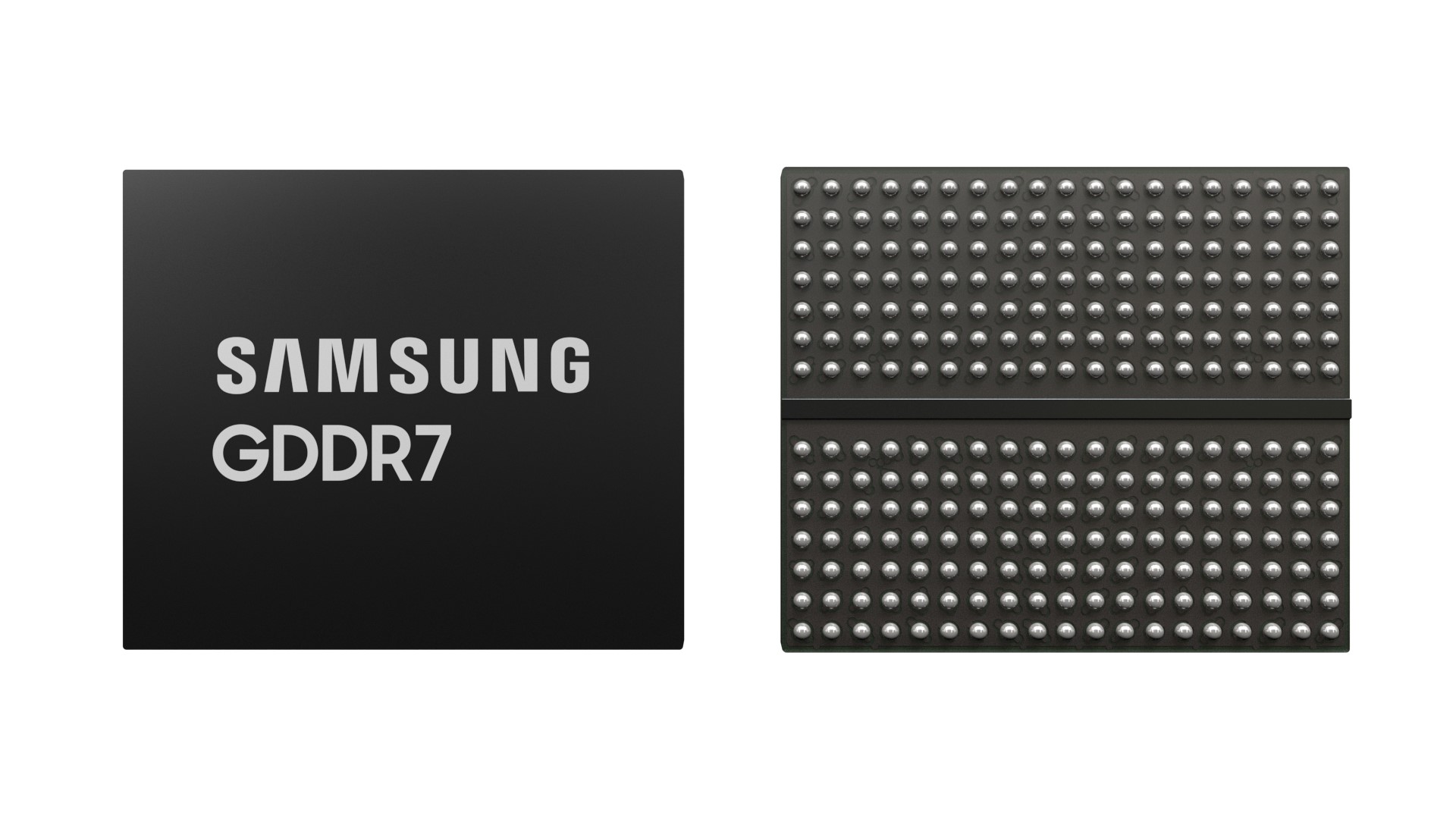
GDDR7 is the newest graphics memory standard from JEDEC, the chip-standards body that also defines GDDR6 and system RAM like DDR5. Published as JESD239 in March 2024, GDDR7 replaces GDDR6's two-bit NRZ signaling with three-level PAM3 encoding, doubles the number of independent memory channels per chip from two to four, and raises the JEDEC-defined bandwidth ceiling to up to 192 GB/s per device. It already ships inside Nvidia's RTX 50-series graphics cards, with Samsung, SK hynix and Micron all building chips for it.
This explainer covers what actually changed between GDDR6 and GDDR7, how the PAM3 encoding and four-channel architecture work, which GPUs use GDDR7 today, and where the three big memory makers stand on production.
- Standard: JEDEC JESD239, published March 5, 2024
- Encoding: PAM3 (3 levels, 3 bits per 2 cycles) replaces GDDR6's NRZ (2 bits per 2 cycles)
- Channels: 4 independent channels per device, up from 2 in GDDR6
- Bandwidth: up to 192 GB/s per device at the JEDEC-defined ceiling
- Shipping GPUs: Nvidia's full RTX 50-series lineup (RTX 5090, 5080, 5070 Ti, 5070)
- Chip makers: Samsung, SK hynix and Micron have all announced GDDR7 production
What is GDDR7?
GDDR7, short for Graphics Double Data Rate 7, is a type of synchronous graphics RAM (SGRAM) standardized by JEDEC specifically for graphics cards, GPUs and other bandwidth-hungry accelerators. JEDEC published the formal specification, JESD239, on March 5, 2024, describing it as a "cutting-edge standard to enhance memory performance in graphics, gaming and AI." It is a free download from JEDEC's own site, like all JEDEC standards.
GDDR7 is not a replacement for the DDR memory in your PC or laptop's system RAM. It is designed to sit on a graphics card or GPU package, wired directly to the GPU die over a wide, short, high-speed bus. If you're looking for what's changing in system memory instead, Pandromeda has a separate explainer on DDR6 RAM, a different standard entirely.
JEDEC's own announcement credits GDDR7 as "the first JEDEC standard DRAM to use the Pulse Amplitude Modulation (PAM) interface," and the standard was developed with direct input from AMD, Nvidia, Samsung, SK hynix and Micron, all of whom are quoted in JEDEC's publication announcement.
GDDR7 vs. GDDR6: the headline numbers
The table below lines up the core specification differences between GDDR7 (JESD239) and GDDR6 (JESD250), based on JEDEC's own publication materials and figures that Samsung has published for its shipping chips of each generation.
| Spec | GDDR6 | GDDR7 |
|---|---|---|
| JEDEC standard | JESD250 | JESD239 |
| Signal encoding | NRZ (2 levels, 2 bits per 2 cycles) | PAM3 (3 levels, 3 bits per 2 cycles) |
| Independent channels per device | 2 | 4 |
| JEDEC-published bandwidth ceiling | not published in the same per-device terms by JEDEC's GDDR7 announcement | up to 192 GB/s per device |
| Fastest shipping per-pin speed (Samsung) | 24 Gbps (Samsung, 2022) | 40–42.5 Gbps (Samsung 24Gb part, 2024) |
| First-generation per-pin speed | 14 Gbps (2018 launch parts, per Wikipedia) | 32 Gbps (Samsung/SK hynix 2023–2024 parts) |
| Samsung-cited system bandwidth example | 1.1 TB/s | 1.5 TB/s at 32 Gbps (1.4x GDDR6) |
| Densities supported | 8–16 Gb typical | 16–32 Gb (JEDEC spec); Samsung has sampled 24 Gb |
| On-die ECC | Not standard | Yes (ODECC with real-time reporting) |
The single most important shift is the move from NRZ to PAM3 signaling, which is what makes everything else in that table possible.
PAM3 encoding: the real change behind GDDR7
GDDR6 uses NRZ (non-return-to-zero) signaling, where each symbol on the data line carries a single bit: the line is either high or low. GDDR7 switches to PAM3, which JEDEC describes as using "3 levels (+1, 0, -1) to transmit 3 bits over 2-cycles versus the traditional NRZ interface transmitting 2 bits over 2-cycles." That extra voltage level lets each clock cycle carry more information without a proportional increase in raw signaling frequency, which in turn helps control power and electromagnetic interference at high speeds.
Samsung's own explanation of its first GDDR7 chips, announced in July 2023, frames the benefit the same way: PAM3 "allows 50% more data to be transmitted than NRZ within the same signaling cycle." JEDEC's announcement also credits PAM3 with improving signal-to-noise ratio "for high frequency operation while enhancing energy efficiency," and notes that JEDEC Board Chairman Mian Quddus called the move to PAM3 signaling a path "to extend the performance of GDDR devices and drive the ongoing evolution of graphics and various high-performance applications."
It's worth distinguishing GDDR7's PAM3 from GDDR6X's PAM4 signaling, a non-JEDEC-standardized scheme Micron co-developed with Nvidia for cards like the GeForce RTX 3080 and 3090. PAM4 uses four voltage levels to carry two bits per symbol; PAM3's three levels carry three bits across two cycles instead. GDDR7 is the first graphics memory scheme in that family to become an actual JEDEC standard rather than a vendor-specific variant.
Four channels instead of two
Alongside the encoding change, JEDEC's GDDR7 standard doubles the number of independent channels inside each memory device, from two in GDDR6 to four in GDDR7. JEDEC's own wording in its publication announcement is direct: the standard "doubles the number of independent channels... from 2 in GDDR6 to 4 in GDDR7." More independent channels mean the memory controller can issue more separate, concurrent commands to the same physical chip, which helps keep the wider PAM3 pipe fed and reduces the chance that one access pattern stalls another.
JEDEC's spec also adds a 2-channel mode for GDDR7, intended to let system designers double effective system capacity where that trade-off against per-channel parallelism makes sense, and supports device densities from 16 Gb to 32 Gb at launch, with Samsung having already sampled a 24 Gb part built on a newer process node.
Bandwidth and per-pin speeds
JEDEC's own figure for GDDR7 is "double the bandwidth over GDDR6, reaching up to 192 GB/s per device." That per-device number assumes a 32-bit-wide device running near the top of GDDR7's data-rate range. According to Wikipedia's GDDR7 entry, the standard has headroom for data rates up to 48 Gbps per pin, though the earliest production chips from Samsung and SK hynix shipped around 32 Gbps per pin in 2023 and 2024, with both companies since announcing faster parts.
Samsung's first GDDR7 chips, announced in July 2023, ran at up to 32 Gbps per pin and delivered what the company described as 1.5 terabytes per second of system-level bandwidth — 1.4 times GDDR6's 1.1 TB/s on a comparable bus, and a 20% improvement in energy efficiency over GDDR6. By October 2024, Samsung said its newer 24 Gb GDDR7 part reached 40 Gbps per pin, with "performance... further enhanced to up to 42.5Gbps, depending on the usage environment," a 25% jump over its first-generation 32 Gbps chips, built using what Samsung calls "5th-generation 10-nanometer (nm)-class DRAM."
SK hynix announced its own GDDR7 in mid-2024, citing a 32 Gbps data rate that it said is "over 60% faster than the previous generation," with headroom to 40 Gbps "depending on conditions." The company's newsroom later detailed engineering work behind that speed, including a T-coil inductor integrated into a mass-produced DRAM chip for the first time at SK hynix, intended to widen the data "eye" margin at high frequencies, plus thermal packaging changes that SK hynix says cut thermal resistance by 74% compared with the prior generation.
Micron is also building GDDR7, and its engineer Frank Ross is quoted directly in JEDEC's GDDR7 publication announcement describing Micron's role in "driving GDDR7 standardization activities with our partners and customers" through "the development of GDDR products utilizing multi-level signaling."
Reliability features: on-die ECC and more
GDDR7 is also the first GDDR generation to build in a serious set of reliability, availability and serviceability (RAS) features as part of the core JEDEC standard, rather than leaving error handling to individual vendors. JEDEC's announcement lists on-die ECC (ODECC) with real-time reporting, data poisoning, error check and scrub, and command/address parity with command blocking (CAPARBLK) as standard GDDR7 features. JEDEC GDDR Subcommittee Chair Michael Litt framed this as a deliberate shift: GDDR7 is "the first GDDR that not only focuses on bandwidth but addresses the market needs for RAS... that allow GDDR devices to better service existing markets such as Cloud gaming and compute and extend into new applications such as AI."
That emphasis on reliability features, alongside raw speed, reflects GDDR7's intended reach beyond gaming graphics cards and into AI inference, high-performance computing and data center accelerators — markets where a memory error has a much higher cost than in a gaming session.
Which GPUs use GDDR7 today
Nvidia's current GeForce RTX 50-series lineup, built on its Blackwell architecture, uses GDDR7 across the board, according to Nvidia's own product pages:
| GPU | Memory | Memory bus width |
|---|---|---|
| GeForce RTX 5090 | 32 GB GDDR7 | 512-bit |
| GeForce RTX 5080 | 16 GB GDDR7 | 256-bit |
| GeForce RTX 5070 Ti | 16 GB GDDR7 | 256-bit |
| GeForce RTX 5070 | 12 GB GDDR7 | 192-bit |
Nvidia's own RTX 5090 product page lists the card's standard memory configuration as "32 GB of super-fast GDDR7 memory" across a 512-bit memory interface; the RTX 5070 and RTX 5070 Ti family page confirms their respective 12 GB and 16 GB GDDR7 configurations. For more on where the flagship card stands amid Nvidia's current product lineup, see Pandromeda's separate coverage of the RTX 5090's status and what Nvidia has and hasn't confirmed. Nvidia itself is also a named contributor to the GDDR7 standard: VP of GPU Product Management Kaustubh Sanghani is quoted in JEDEC's publication announcement saying Nvidia's work with JEDEC "helped to make PAM signaling the foundational technology for GDDR7, helping customers to get the most performance out of their GPU."
Who makes GDDR7: Samsung, SK hynix and Micron
All three major DRAM makers build GDDR7, and all three were directly involved in the JEDEC standardization process:
- Samsung announced what it called the industry's first GDDR7 DRAM in July 2023, a 16 Gb part at up to 32 Gbps, and followed up in October 2024 with a 24 Gb part reaching 40 Gbps (up to 42.5 Gbps), aimed at both graphics cards and AI workstations.
- SK hynix introduced its GDDR7 in mid-2024 at up to 40 Gbps, and has since published engineering detail on the T-coil inductor and thermal packaging work that got it there, framing GDDR7 as relevant to "AI, high-performance computing (HPC), and autonomous driving" as well as graphics.
- Micron is also a GDDR7 supplier and, per JEDEC's own publication announcement, played what the company describes as "a critical role in driving GDDR7 standardization activities" through its work on multi-level signaling for graphics DRAM.
At JEDEC's GDDR7 launch, Samsung's YongCheol Bae, EVP of Memory Product Planning, said "GDDR7 32Gbps will achieve 1.6x higher-performance with the highest reliability and cost-effectiveness," while SK hynix VP of Product Planning Sang Kwon Lee called the standardization work "a new opportunity for the industry to expand the memory ecosystem."
GDDR7 vs. other memory types
It's easy to conflate GDDR7 with other next-generation memory standards making headlines at the same time, but they serve different jobs. GDDR7 is graphics memory: soldered directly onto a GPU board, optimized for high per-pin bandwidth over a relatively short, wide bus to a single GPU die. HBM4, by contrast, is a stacked, 3D high-bandwidth memory standard aimed primarily at AI accelerators and data-center GPUs, where even higher aggregate bandwidth per watt matters more than per-pin speed. Meanwhile, standards like DDR6 and the CAMM2 module format address an entirely different problem: general-purpose system memory for CPUs in PCs and servers, not GPU-attached graphics memory. None of these standards are interchangeable, and a GPU vendor's choice between them comes down to cost, board space, power budget and target bandwidth per chip.
What's next for GDDR7
With JESD239 finalized and Samsung, SK hynix and Micron all shipping or sampling parts, the near-term trajectory for GDDR7 is incremental: faster per-pin speeds climbing toward the JEDEC-permitted ceiling, higher-density single chips (Samsung's 24 Gb part being the first public example beyond JEDEC's initial 16–32 Gb range), and broader adoption outside Nvidia's RTX 50 series as more GPU and accelerator vendors design around the standard. JEDEC's own RAS feature set — on-die ECC, data poisoning, and command/address parity — also signals that GDDR7 is being positioned for AI and data-center workloads, not just gaming graphics cards, which could widen where the standard shows up over the next few product cycles. Watch for JEDEC revisions to the published JESD239 standard and for official per-pin speed confirmations from Samsung, SK hynix and Micron as production matures.
Frequently asked questions
What is GDDR7?
GDDR7 is the latest JEDEC graphics memory standard, published as JESD239 in March 2024. It's designed for GPUs and graphics cards rather than system RAM, and it replaces GDDR6's NRZ signaling with PAM3 encoding for higher bandwidth.
How is GDDR7 different from GDDR6?
GDDR7 uses three-level PAM3 signaling instead of GDDR6's NRZ, doubles independent memory channels from 2 to 4 per device, and raises JEDEC's per-device bandwidth figure to up to 192 GB/s, while adding standard on-die ECC that GDDR6 lacked.
Which graphics cards use GDDR7?
Nvidia's entire GeForce RTX 50-series lineup uses GDDR7, including the RTX 5090 (32GB, 512-bit bus), RTX 5080 (16GB, 256-bit), RTX 5070 Ti (16GB, 256-bit) and RTX 5070 (12GB, 192-bit), according to Nvidia's own product pages.
Is GDDR7 the same as GDDR6X?
No. GDDR6X is a proprietary scheme Micron co-developed with Nvidia that uses PAM4 signaling and was never standardized by JEDEC. GDDR7 is a full JEDEC standard (JESD239) that uses PAM3 signaling instead.
Who manufactures GDDR7 memory chips?
Samsung, SK hynix and Micron all produce GDDR7. Samsung announced the first GDDR7 chips in July 2023, SK hynix introduced its version in mid-2024, and Micron also contributed to the JEDEC standardization process through its work on multi-level signaling.
How fast is GDDR7 compared to GDDR6?
JEDEC says GDDR7 offers double the bandwidth of GDDR6, reaching up to 192 GB/s per device. Samsung's first GDDR7 chips ran at up to 32 Gbps per pin versus 24 Gbps for its fastest shipping GDDR6, and Samsung's newer 24Gb GDDR7 parts reach 40-42.5 Gbps.
Sources
- JEDEC – JESD239 GDDR7 Publication Announcementjedec.org
- Samsung Newsroom – Industry's First GDDR7 DRAM (July 2023)news.samsung.com
- Samsung Newsroom – Industry's First 24Gb GDDR7 DRAM (October 2024)news.samsung.com
- SK hynix Newsroom – GDDR7 Design Innovationsnews.skhynix.com
- Nvidia – GeForce RTX 5090 Specificationsnvidia.com
- Wikipedia – GDDR7 SDRAMen.wikipedia.org
Mara Lindqvist edits the hardware desk. She covers graphics cards, processors, memory and storage, the foundries and chip designers behind them, and what the numbers on a spec sheet mean for people choosing a PC. Specifications in her stories come from manufacturer spec pages and datasheets.