HBM4 Explained: Bandwidth, Makers and HBM4 vs HBM4E
HBM4 is JEDEC's newest stacked memory standard for AI accelerators. Here is what its real bandwidth, makers, and roadmap mean for GPU and RAM prices.
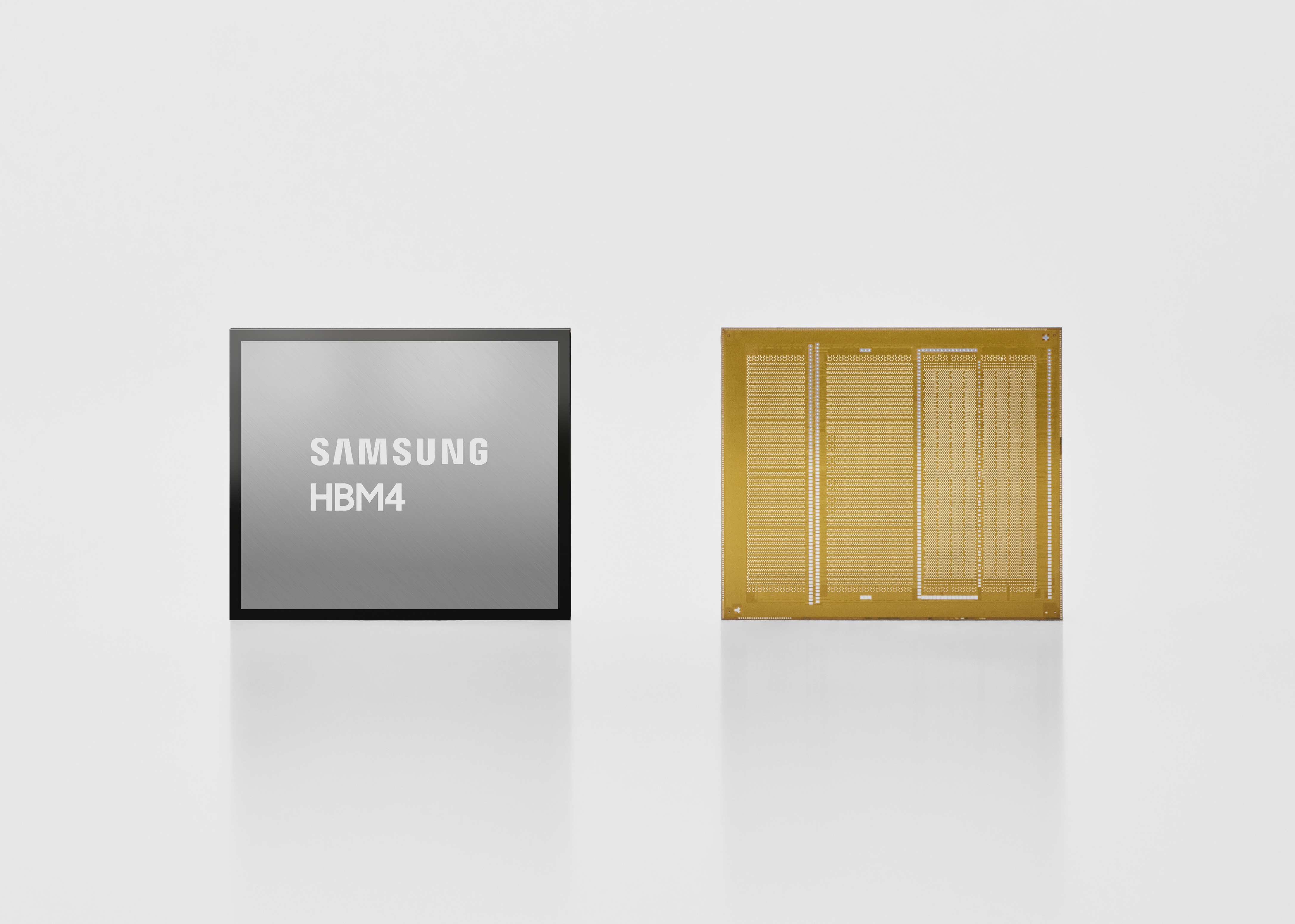
HBM4 is the fourth generation of High Bandwidth Memory, the stacked DRAM standard that sits directly on top of AI accelerators and high-end GPUs instead of living on a separate circuit board. JEDEC finalized the HBM4 standard (JESD270-4) in April 2025 with a 2,048-bit interface per stack — double the width of HBM3E — and a baseline data rate of up to 8 gigabits per second (Gb/s) per pin, for a JEDEC-spec bandwidth of up to 2 terabytes per second (TB/s) per stack. SK hynix, Samsung and Micron have each said their real shipping HBM4 runs faster than that JEDEC floor, and the memory is built for next-generation AI GPUs such as Nvidia's Vera Rubin platform, not for a desktop PC you can buy at retail.
HBM4 quick facts
- Standard: JEDEC JESD270-4, published April 2025
- Interface width: 2,048-bit per stack (vs. 1,024-bit for HBM3E)
- JEDEC baseline speed: up to 8 Gb/s per pin, up to 2 TB/s per stack
- Real shipping speeds: 10+ Gb/s (SK hynix), 11.7–13 Gb/s (Samsung), 11+ Gb/s (Micron)
- Makers: SK hynix, Samsung, Micron — all three sampling or shipping as of early 2026
- First customer platform named by suppliers: Nvidia's Vera Rubin AI GPU
- Sold to: chipmakers and AI accelerator builders, not retail consumers
What is HBM4?
HBM4 (High Bandwidth Memory, 4th generation) is a type of stacked DRAM: multiple memory dies are bonded vertically into a single package and connected to a logic base die, which in turn sits next to a GPU or AI accelerator die on the same silicon interposer. Because the memory is physically close to the processor and uses an extremely wide interface, it moves far more data per second than conventional system memory, at the cost of capacity and cost per gigabyte. HBM4 is the successor to HBM3E and is governed by the JEDEC JESD270-4 standard, which JEDEC published in April 2025 after collaborating with memory makers and AI chip designers.
HBM4 is not a replacement for the DRAM in your laptop or phone. It is used exclusively inside data-center AI accelerators, high-performance computing (HPC) processors, and the highest-end professional GPUs. If you want to read about the memory standards that actually ship inside consumer PCs, Pandromeda has already covered DDR6 system RAM and the compact CAMM2 module format — both are a completely different, unrelated product category from HBM4. For a broader primer on stacked memory in general, see Wikipedia's High Bandwidth Memory entry, which also covers earlier HBM, HBM2 and HBM3 generations.
How HBM4 differs from HBM3E
The single biggest architectural change in HBM4 is interface width. JEDEC doubled the number of data channels per stack from 16 in HBM3 to 32 independent channels (each split into two pseudo-channels) in HBM4, which doubles the physical interface from 1,024 bits to 2,048 bits. That alone roughly doubles bandwidth at a given per-pin data rate, even before any speed increase. The JESD270-4 standard also lets manufacturers choose from several VDDQ voltage levels (0.7V, 0.75V, 0.8V or 0.9V) to tune power efficiency, and it keeps HBM4 logically compatible with the kind of controller designs built for HBM3, which shortens the integration work for chip designers moving to the new standard.
On top of the JEDEC floor, every major supplier has pushed real shipping parts well past the 8 Gb/s baseline. SK hynix said its HBM4 reaches operating speeds above 10 Gb/s per pin — about 25% above the JEDEC spec — and that the combination of the wider interface and higher speed roughly doubles bandwidth versus HBM3E while cutting power use by more than 40%. Samsung's commercial HBM4, which it began shipping in February 2026, runs at a consistent 11.7 Gb/s (scalable to 13 Gb/s), which the company says is about 46% above the 8 Gb/s JEDEC standard and raises per-stack bandwidth by 2.7x versus HBM3E to as much as 3.3 TB/s. Micron's HBM4 36GB parts, shipped in volume from Q1 2026, run above 11 Gb/s per pin for more than 2.8 TB/s of bandwidth per stack — a 2.3x jump over its own HBM3E.
HBM4 bandwidth and speed specs
"HBM4 bandwidth" does not have one single number, because JEDEC sets a floor and each supplier then qualifies its own parts to run faster. Here is how the JEDEC baseline compares with what SK hynix, Samsung and Micron have each confirmed for shipping or sampled HBM4, alongside the preceding HBM3E generation and the early HBM4E follow-on.
| Standard / part | Interface width | Data rate per pin | Max bandwidth per stack | Stack height |
|---|---|---|---|---|
| HBM3E (prior gen) | 1,024-bit | up to ~9.8 Gb/s | ~1.2 TB/s | 8–12-layer |
| HBM4 — JEDEC JESD270-4 baseline | 2,048-bit | up to 8 Gb/s | up to 2 TB/s | 4–16-layer |
| HBM4 — SK hynix (shipping) | 2,048-bit | 10+ Gb/s | ~2.5+ TB/s | 12-layer, 36GB |
| HBM4 — Samsung (shipping) | 2,048-bit | 11.7 Gb/s (up to 13) | up to 3.3 TB/s | 12-layer |
| HBM4 — Micron (shipping) | 2,048-bit | 11+ Gb/s | 2.8+ TB/s | 12-layer, 36GB; 16-layer, 48GB samples |
| HBM4E — Samsung (sampling) | 2,048-bit | 14 Gb/s (up to 16) | up to 3.6 TB/s | 12-layer, with 16-layer planned |
In every case, a GPU package uses several HBM4 stacks at once, so the bandwidth delivered to the processor is a multiple of the per-stack figure above — stacking eight HBM4 packages, for example, multiplies whichever per-stack number a given chip design uses by eight.
Who makes HBM4: SK hynix, Samsung and Micron
All three of the world's major DRAM makers are now building HBM4, and each has described its own milestones:
- SK hynix says it was the first company to complete HBM4 development and prepare mass production, reaching that milestone in September 2025 after shipping initial 12-layer HBM4 samples in March 2025. Its process combines advanced mass reflow molded underfill (MR-MUF) packaging with 10nm-class "1b" (fifth-generation 10nm) DRAM, and it is working with TSMC on the logic base die.
- Samsung announced in February 2026 that it had begun mass production and commercial shipment of HBM4, pairing its DRAM with a 4-nanometer logic base die built on its own foundry process. Samsung has said it expects total HBM sales to more than triple in 2026 versus 2025 as HBM4 ramps, and by mid-2026 it had also started sampling 12-layer HBM4E parts to customers.
- Micron shipped its first HBM4 36GB 12-high samples in June 2025 and moved to volume shipment of that same part in the first quarter of 2026, explicitly naming Nvidia's Vera Rubin platform as a target design. Micron has also sampled a denser 48GB, 16-die HBM4 stack and is working with TSMC on the logic base die for its next-generation HBM4E, due in 2027.
Nvidia, AMD and the other major buyers of HBM4 do not manufacture the memory themselves — they qualify and buy finished stacks from SK hynix, Samsung and Micron, which is why all three suppliers' press releases talk about customer qualification and sample shipments rather than retail availability.
Which chips and GPUs use HBM4
HBM4 is built for AI accelerators and HPC processors, not gaming GPUs. The most frequently named customer platform across all three suppliers' own announcements is Nvidia's next-generation Vera Rubin AI GPU family, which Micron explicitly cited as the target for its volume HBM4 shipments starting in Q1 2026. SK hynix and Samsung have likewise discussed supplying HBM4 for "next-generation AI platforms" without committing every spec to a single customer in writing, since exact stack counts and speed bins are set by each chip designer's own qualification process. AMD's Instinct accelerator line is also expected to move to HBM4 on a similar timeline, following the same industry-wide generational shift away from HBM3E.
Because HBM4 only ships inside accelerators that themselves cost many thousands of dollars and sell to cloud providers and AI labs rather than consumers, there's no retail "HBM4 price" the way there's a price for a stick of RAM — it's a component cost baked into the AI chip itself, set through direct negotiation between chipmakers and the three memory suppliers.
HBM4 vs HBM4E
HBM4E is the planned mid-generation speed bump on top of HBM4, in the same way HBM3E followed HBM3. It keeps the same 2,048-bit interface JEDEC defined for HBM4 but targets meaningfully higher per-pin data rates. Samsung's HBM4E samples, shipped from around mid-2026, run at a stable 14 Gb/s (scalable to 16 Gb/s) — more than 20% faster than its own HBM4 — for up to 3.6 TB/s of bandwidth per stack, and the company has outlined plans for a denser 16-layer HBM4E on top of its initial 12-layer samples. Micron has said its own HBM4E, developed with a TSMC-built logic base die, is aimed at a 2027 launch. In short: HBM4 is the generation now reaching GPUs in 2026, and HBM4E is the faster refinement suppliers are already sampling for AI chips expected in 2027 and beyond.
HBM4 vs GDDR7: different jobs, not direct competitors
GDDR7 is the memory standard JEDEC finalized for mainstream and high-end graphics cards — the type of chip soldered around the edge of a GPU board rather than stacked on top of it. GDDR7 uses PAM3 signaling and launches at roughly 32 Gb/s per pin, which is far higher per-pin than HBM4, but GDDR7 chips are not stacked and each one connects over a much narrower interface, so a graphics card needs many separate GDDR7 chips around the GPU die to approach the bandwidth a handful of stacked HBM4 packages deliver right next to the processor. In practice, GDDR7 is built for cost-sensitive, mass-market graphics cards, while HBM4 is built for capacity- and bandwidth-hungry AI accelerators where the extra manufacturing cost of 3D stacking is worth it. The two standards serve different markets rather than competing head-to-head on the same products — mainstream gaming GPUs use GDDR7 (see Wikipedia's GDDR7 SDRAM entry for the full spec history), not HBM4.
HBM4 and the broader chip and RAM price story
HBM4 does not have a consumer price tag — it's sold directly to chipmakers like Nvidia and AMD, not through retail channels, and none of SK hynix, Samsung or Micron has published a per-unit price for HBM4 stacks. What all three suppliers have said is that HBM4 carries a higher manufacturing cost than HBM3E, driven by the wider 2,048-bit interface, taller stacks, and in Samsung's case a logic base die built on an advanced foundry node, and that demand is intense enough that Samsung expects its total HBM revenue to more than triple in 2026. That supply squeeze is part of the same underlying dynamic Pandromeda covered when AMD and Intel raised chip prices in Q4 2026: DRAM fabs that shift wafer capacity toward higher-margin HBM4 for AI customers have less capacity left for conventional DRAM, which is a contributing factor in the mainstream RAM price increases that have also hit system memory and laptop pricing. If you're tracking "HBM4 stock" in the sense of memory-maker shares rather than retail inventory, that capacity reallocation and the race to qualify with Nvidia are the two forces analysts and the companies themselves point to most often.
HBM4 timeline so far
| Date | Milestone |
|---|---|
| April 2025 | JEDEC publishes the JESD270-4 HBM4 standard |
| March 2025 | SK hynix ships initial 12-layer HBM4 samples to customers |
| June 2025 | Micron ships HBM4 36GB 12-high samples to key customers |
| September 2025 | SK hynix says it completed HBM4 development and readied mass production, the first supplier to do so |
| Q1 2026 | Micron begins volume shipment of HBM4 36GB 12-high, naming Nvidia's Vera Rubin as a target platform |
| February 2026 | Samsung begins mass production and commercial shipment of HBM4 |
| Mid-2026 onward | Samsung begins sampling 12-layer HBM4E; Micron targets HBM4E for 2027 |
Common questions about HBM4
HBM4 searches cluster around a handful of recurring questions, which is a good sign of exactly how unfamiliar — and how commercially important — this memory standard has become outside of chip-industry circles. The FAQ section below covers the most common ones directly.
What to watch next
The next concrete milestones worth tracking are Nvidia's own confirmation of final HBM4 stack counts and speed bins for shipping Vera Rubin hardware, Samsung's move from sampling to shipping 12-layer HBM4E, and whether SK hynix, Samsung or Micron publish updated capacity or revenue guidance tied specifically to HBM4 in their next quarterly earnings calls. Because none of the three suppliers report a retail HBM4 price, the clearest public signal of how tight supply remains will keep coming from their revenue mix disclosures and from how much further mainstream DRAM and laptop pricing moves alongside it.
Frequently asked questions
What is HBM4?
HBM4 (High Bandwidth Memory, 4th generation) is the JEDEC-standardized stacked DRAM used in AI accelerators and HPC processors. It uses a 2,048-bit interface per stack, double HBM3E's width, and JEDEC's JESD270-4 standard sets a baseline of up to 8 Gb/s per pin for up to 2 TB/s of bandwidth per stack.
What is HBM4's real bandwidth?
JEDEC's spec floor is up to 2 TB/s per stack, but suppliers ship faster: SK hynix's HBM4 runs above 10 Gb/s per pin, Samsung's runs at 11.7-13 Gb/s for up to 3.3 TB/s per stack, and Micron's runs above 11 Gb/s for more than 2.8 TB/s per stack.
Who makes HBM4?
The three major DRAM makers — SK hynix, Samsung, and Micron — all design and manufacture HBM4. SK hynix said it completed development and readied mass production first, in September 2025; Samsung began commercial shipment in February 2026; Micron moved to volume shipment of its HBM4 36GB part in Q1 2026.
Which chips use HBM4?
HBM4 is built for AI accelerators and HPC processors, not consumer GPUs. Micron has named Nvidia's Vera Rubin AI GPU platform as a target design for its volume HBM4 shipments, and AMD's Instinct accelerator line is expected to adopt HBM4 on a similar timeline.
What is HBM4E, and how is it different from HBM4?
HBM4E is the planned speed-bumped follow-on to HBM4, using the same 2,048-bit interface but targeting higher per-pin data rates. Samsung's HBM4E samples run at 14 Gb/s (up to 16 Gb/s), more than 20% faster than its HBM4, for up to 3.6 TB/s per stack.
What does HBM4 cost?
There is no published retail or per-unit price for HBM4 — it is sold directly by SK hynix, Samsung, and Micron to chipmakers like Nvidia and AMD, not through retail channels. All three suppliers have said HBM4 costs more to manufacture than HBM3E, which is a factor in tighter DRAM supply overall.
Sources
- JEDEC: JESD270-4 HBM4 Standard Releasebusinesswire.com
- SK hynix Newsroom: HBM4 Mass Productionnews.skhynix.co.kr
- Samsung Newsroom: Industry-First Commercial HBM4news.samsung.com
- Micron: HBM4 Press Release (Investor Relations)micron.gcs-web.com
- Wikipedia: High Bandwidth Memoryen.wikipedia.org
- Wikipedia: GDDR7 SDRAMen.wikipedia.org
Mara Lindqvist edits the hardware desk. She covers graphics cards, processors, memory and storage, the foundries and chip designers behind them, and what the numbers on a spec sheet mean for people choosing a PC. Specifications in her stories come from manufacturer spec pages and datasheets.