Chiplet Design Explained: Why Modern Chips Are Built From Tiles
Modern CPUs and AI accelerators are no longer single slabs of silicon. Here is what a chiplet actually is, how the pieces connect, and why the whole industry moved to tiles.
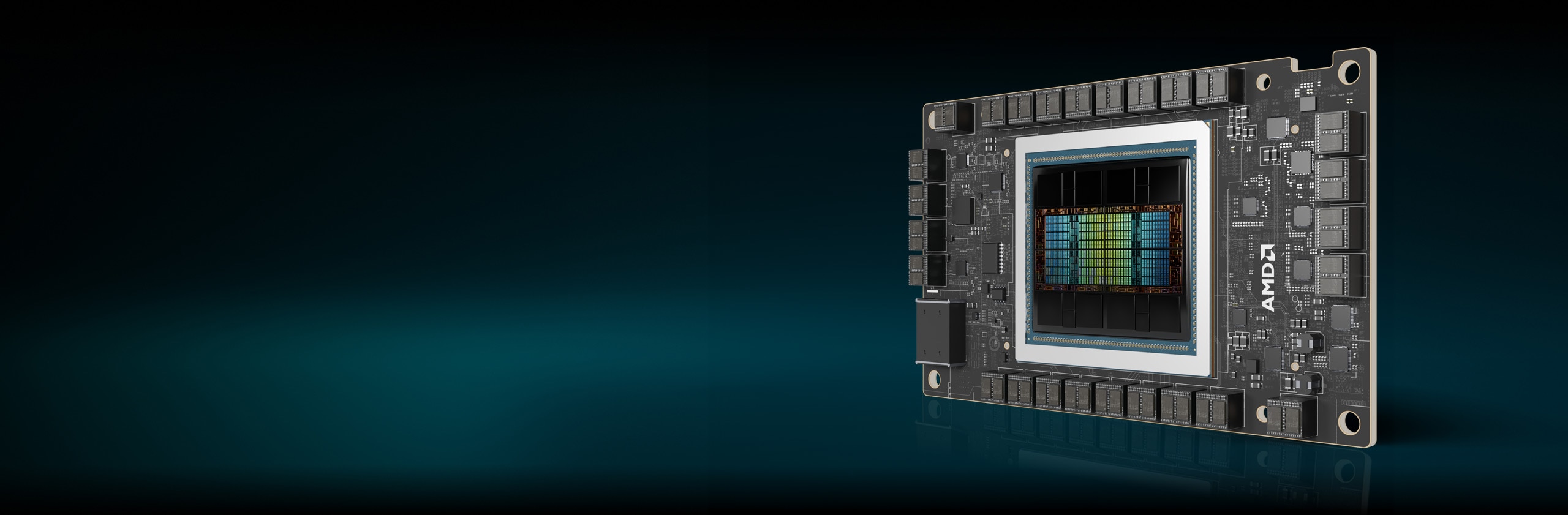
A chiplet is a small, self-contained piece of a larger chip — a single function, such as CPU cores, graphics compute, I/O, or cache, built as its own tiny die and then wired together with other chiplets inside one package. Instead of etching an entire processor onto one giant slab of silicon (a "monolithic" die), chipmakers now cut the design into several smaller dies, build each on whichever manufacturing process suits it best, and glue the results together with a high-speed interconnect. It's the reason AMD's Ryzen and EPYC chips, Intel's Meteor Lake and Arrow Lake processors, and Nvidia's newest AI accelerators are all, physically, several chips wearing a single chip's nameplate.
- A chiplet is one function (cores, I/O, cache, graphics) made as its own small die, not a whole processor by itself.
- Multiple chiplets are combined in one package using 2.5D or 3D packaging — interposers, bridges, or direct die-on-die stacking.
- Chiplets talk to each other over dense, short-reach interconnects: AMD's Infinity Fabric, Intel's EMIB/Foveros, Nvidia's NVLink-C2C, or the open UCIe standard.
- The appeal is mostly economic: smaller dies have far better manufacturing yield than one huge die, and each chiplet can be built on whichever process node actually needs it.
- The cost is latency, power, and packaging complexity that a single monolithic die never has to deal with.
What exactly is a chiplet?
According to the engineering definition, a chiplet is "a small integrated circuit that contains a well-defined subset of functionality" that gets combined with other chiplets on an interposer to form a larger, more complex chip, as Wikipedia's chiplet entry describes it. The term itself dates back to 2006, coined by UC Berkeley professor John Wawrzynek as part of an academic multiprocessor research project, long before it became an industry buzzword.
The practical distinction that matters: a chiplet is not a finished product on its own. A Zen 5 "core complex die" (CCD) from AMD, for instance, is useless without the separate I/O die it plugs into — it has cores and cache, but no memory controller or PCIe lanes of its own. The chiplet is a building block, not a chip in the traditional sense.
Chiplets vs. a monolithic die
A monolithic chip puts every function — CPU cores, memory controllers, I/O, sometimes graphics — on one continuous piece of silicon, cut from a single wafer in a single process. That's how essentially every processor was built until the last decade or so, and it's still how many simpler chips are made today.
Chiplet-based design splits those functions across multiple dies that are manufactured separately — potentially in different fabs, on different process nodes, even by different companies — and then assembled into one package afterward. Wikipedia's entry lists the three advantages this is meant to buy: chiplets can be reused across multiple products, different chiplets can use whichever process node or material suits their job (a practice called heterogeneous integration), and each individual chiplet can be tested before it's committed to an expensive final assembly, which improves the yield of the finished part.
The drawbacks run the other way: power density goes up, which means more aggressive cooling, and getting reliable, high-bandwidth communication between dies — especially dies from different vendors — is a genuinely hard engineering problem that a single piece of silicon never has to solve.
Why the chip industry moved to tiles
The driving force is yield economics. As process nodes shrink, the odds that a random manufacturing defect lands somewhere on a given chip go up with the chip's physical area — a bigger die has more silicon for a flaw to hit, and one bad spot can ruin the whole part. Cut that same design into several smaller dies, and a single defect only kills one small chiplet instead of an entire multi-hundred-square-millimeter processor; the rest of the chiplets on that wafer are still salvageable. Smaller dies are also cheaper to manufacture per unit, and defective ones are a much smaller loss when they do turn up.
AMD's own account of its chiplet strategy, laid out in its chiplet architecture white paper, points to a second factor: not every part of a processor benefits equally from a new, expensive process node. Physical interfaces like memory controllers and I/O don't shrink as efficiently as compute logic does, so AMD's first Zen 2-generation EPYC and Ryzen chips, launched in 2019, split the design into compute chiplets built on a (then cutting-edge) 7nm process and a separate I/O die built on a cheaper, more mature 14nm process. Each piece gets exactly the process it needs — no more, no less.
How chiplets actually talk to each other
None of this works without a fast, dense, low-latency link between dies that are physically separate but need to act like one chip. Each major vendor built its own proprietary interconnect for this before any of them tried to standardize:
- AMD Infinity Fabric / Infinity Architecture connects AMD's CPU and GPU chiplets, both within a package and, in its newer "Infinity Architecture" form, across multiple chips in a system.
- Intel EMIB (Embedded Multi-die Interconnect Bridge) embeds small silicon bridges directly into the package substrate, wherever two dies need to connect, rather than using one large interposer under the whole package. Intel has shipped EMIB since 2017.
- Intel Foveros goes a step further and stacks chiplets vertically — one die on top of another — rather than placing them side by side. Intel first demonstrated it commercially in the 2020 Lakefield chip and now uses it in Meteor Lake, Arrow Lake, and Lunar Lake.
- Nvidia NVLink-C2C is Nvidia's own chip-to-chip link, used to fuse its Grace CPU to Blackwell GPUs inside a single superchip module at up to 900 GB/s, according to Nvidia's own technical documentation.
Each of these is proprietary — designed by one company for its own chiplets. That's fine when AMD is only connecting AMD dies to each other, but it's a dead end for an industry that increasingly wants to mix chiplets from different vendors in a single package.
The packaging technology that makes it physically possible
Connecting chiplets electrically is only half the problem; they also have to be physically assembled into one package without the connections between them becoming a bottleneck. TSMC's 3DFabric platform splits this into two categories: front-end 3D stacking, where TSMC's SoIC technology bonds dies directly on top of each other (used for AMD's 3D V-Cache stacked cache dies); and back-end packaging, where the CoWoS family of technologies places multiple dies side-by-side on a shared interposer or substrate.
Intel runs a parallel stack of its own technologies covering similar ground, which its newsroom described in detail in a 2026 overview of its advanced packaging operations: EMIB for bridging dies side-by-side without a full interposer, Foveros for stacking dies vertically, and a newer variant called EMIB-T that routes power directly through the bridge itself rather than around it, aimed at the power delivery demands of chips paired with high-bandwidth memory. Intel says its packaging roadmap is aiming for package sizes roughly 8 times today's reticle limit, scaling toward more than 12 times by 2028.
| Technology | Maker | What it does | Where it's used |
|---|---|---|---|
| Infinity Fabric / Infinity Architecture | AMD | Proprietary die-to-die and system-level interconnect | Ryzen, EPYC, Instinct accelerators |
| EMIB | Intel | Silicon bridge embedded in the substrate, side-by-side dies | Sapphire Rapids, Ponte Vecchio |
| Foveros | Intel | Vertical 3D die stacking | Lakefield, Meteor Lake, Arrow Lake, Lunar Lake |
| CoWoS / SoIC (3DFabric) | TSMC | Interposer-based 2.5D packaging (CoWoS) and direct die stacking (SoIC) | AMD 3D V-Cache, most AI accelerator packages |
| NVLink-C2C | Nvidia | Proprietary high-bandwidth chip-to-chip link, up to 900 GB/s | Grace-Hopper, Grace-Blackwell superchips |
| UCIe | UCIe Consortium (open standard) | Vendor-neutral die-to-die interconnect, 48–64 GT/s in version 3.0 | Intended for cross-vendor chiplet mixing |
UCIe: an attempt at a universal chiplet standard
Universal Chiplet Interconnect Express launched in 2022 as an open, royalty-bearing standard backed by AMD, Intel, Arm, and major foundry partners, built on top of the existing PCI Express and Compute Express Link protocols. The goal is straightforward even if the engineering isn't: let a chiplet designed by one company connect reliably to a chiplet designed by a completely different company, the way a PCIe card from any vendor plugs into any PCIe slot today.
The UCIe Consortium's own specification page lists four released versions. UCIe 1.0 defined the core die-to-die physical layer, protocol stack, and compliance testing. UCIe 1.1 added reliability mechanisms and runtime health monitoring. UCIe 2.0 added management features and support for 3D packaging. UCIe 3.0, the newest version, doubles the previous generation's 32 GT/s data rate to 48–64 GT/s, while staying backward compatible with every earlier version.
Nvidia, notably, didn't join at UCIe's 2022 launch and still leans on its own NVLink-C2C for its highest-performance internal links — but the company has said that custom-silicon partners connecting to its chips can choose either the open UCIe standard or NVLink-C2C, and in 2025 it opened that interconnect more broadly through a program called NVLink Fusion, letting partners including MediaTek, Marvell, and Qualcomm build custom chips that connect into Nvidia's scale-up fabric. Despite the standardization push, most shipping chips today — AMD's EPYC processors, Nvidia's Grace-Hopper superchips — still rely on each company's own proprietary die-to-die link rather than UCIe for their primary internal connections.
Real chips built this way today
Chiplet design stopped being exotic a while ago. AMD has used it continuously since the 2019 debut of Zen 2-based Ryzen 3000 and EPYC "Rome" processors, and its upcoming Zen 6 generation — covered in our look at what's confirmed for Zen 6 — continues splitting compute dies from I/O. AMD's Instinct MI300 series goes further still, combining Zen 4 CPU chiplets with CDNA 3 GPU chiplets and unified HBM3 memory inside one package, with the MI300A variant pairing 24 Zen 4 cores and 228 GPU compute units on a single module, according to AMD's own product specifications.
Intel's chiplet-based ("tile-based," in Intel's own vocabulary) processors include Meteor Lake, Arrow Lake, and the data-center Sapphire Rapids and Ponte Vecchio parts; its next consumer generation, Nova Lake, is expected to extend the same tile approach, as detailed in our Nova Lake release-date roundup. On the process side, the move to denser nodes such as TSMC's N2 — explained in our N2 process explainer — makes individual compute chiplets smaller and more expensive per square millimeter, which only strengthens the yield argument for splitting designs into tiles rather than building one monolithic die at the leading edge.
AI accelerators lean on chiplets the hardest of all, because the alternative — one monolithic die carrying both compute logic and enormous amounts of attached memory — would run straight into the reticle size limits of modern lithography tools. Nvidia's Grace-Blackwell superchips fuse a CPU and GPU die via NVLink-C2C; AMD's MI300-series and upcoming MI400-series accelerators do the equivalent with Infinity Fabric and TSMC's advanced packaging.
The trade-offs nobody skips past
Splitting a chip into pieces doesn't come free. Communication between two separate dies is always slower and higher-latency than communication within a single piece of silicon, no matter how good the interconnect is — Wikipedia's chiplet entry flags this directly as one of the technology's core limitations, alongside the higher power density that stacked or tightly packed dies create, which pushes cooling requirements up. Packaging itself is also a manufacturing step with its own cost and its own chance of failure; a perfectly good chiplet can still be ruined by a bad bonding or stacking step after it leaves the fab. None of this is a reason chiplets fail to make sense — the yield and flexibility math still favors them for large, complex chips — but it's why a basic, inexpensive microcontroller or an entry-level mobile chip is still built as one simple monolithic die rather than a cluster of tiles.
What's next for chiplet design
The near-term trend is more chiplets per package, not fewer. Intel's public packaging roadmap already points toward packages many times larger than today's reticle limit by 2028, built from a growing number of smaller compute and memory tiles. TSMC continues expanding CoWoS capacity specifically to keep up with AI accelerator demand. And UCIe's 3.0 revision, with its doubled data rate, is aimed squarely at closing the performance gap between an open, cross-vendor standard and the proprietary links AMD, Intel, and Nvidia still prefer for their own highest-performance connections.
Whether a genuinely mixed-vendor chiplet — AMD compute paired with a third-party I/O die, say — becomes a mainstream commercial product, or UCIe mainly ends up standardizing interfaces that companies still use only internally, is still an open question. What's not in question is that the "one giant monolithic die" approach is no longer the default for anything at the performance end of the market; it's chiplets from here.
Frequently asked questions
What is a chiplet, in simple terms?
A chiplet is a small chip that handles one specific function — such as CPU cores, graphics, I/O, or cache — and is designed to be combined with other chiplets inside a single processor package, rather than functioning as a complete chip on its own.
How is chiplet design different from a regular, single-die chip?
A traditional monolithic chip puts every function on one continuous piece of silicon. Chiplet design splits those functions across several smaller dies, often built on different manufacturing processes, which are then physically assembled into one package afterward.
Why did AMD, Intel, and Nvidia move to chiplets?
Mainly manufacturing yield economics: smaller dies are far less likely to be ruined by a random defect than one large die, and each chiplet can be built on whichever process node actually benefits its function, rather than forcing an entire chip onto one expensive node.
What is UCIe and why does it matter?
UCIe (Universal Chiplet Interconnect Express) is an open industry standard, backed by AMD, Intel, Arm, and major foundries, meant to let chiplets from different companies connect to each other reliably — the way any PCIe card works in any PCIe slot today. Most shipping chips still use each company's own proprietary interconnect instead.
Do chiplets make chips slower than a monolithic design?
Communication between separate dies is inherently higher-latency than communication within one piece of silicon. Chipmakers offset this with very short, very wide, high-bandwidth interconnects, but it remains one of the genuine trade-offs of chiplet design compared to a monolithic die.
Which products actually use chiplet design today?
AMD's Ryzen, EPYC, and Instinct processors; Intel's Meteor Lake, Arrow Lake, Sapphire Rapids, and Ponte Vecchio chips; and Nvidia's Grace-Hopper and Grace-Blackwell superchips are all built from multiple chiplets rather than a single monolithic die.
Sources
- Wikipedia – Chipleten.wikipedia.org
- UCIe Consortium – Specification versionsuciexpress.org
- AMD – Chiplet Architecture White Paper (PDF)amd.com
- Intel Newsroom – U.S. Advanced Packaging Enables Next-Generation AI Semiconductorsintel.com
- TSMC – 3DFabric HPC Wafer-Level System Integrationtsmc.com
- NVIDIA Investor Relations – NVLink Fusion announcementinvestor.nvidia.com
Mara Lindqvist edits the hardware desk. She covers graphics cards, processors, memory and storage, the foundries and chip designers behind them, and what the numbers on a spec sheet mean for people choosing a PC. Specifications in her stories come from manufacturer spec pages and datasheets.