What Is High Bandwidth Flash (HBF)? The New AI Memory Explained
Sandisk and SK hynix just published the first open technical spec for High Bandwidth Flash, a new NAND-based memory tier between HBM and SSDs built for AI accelerators.
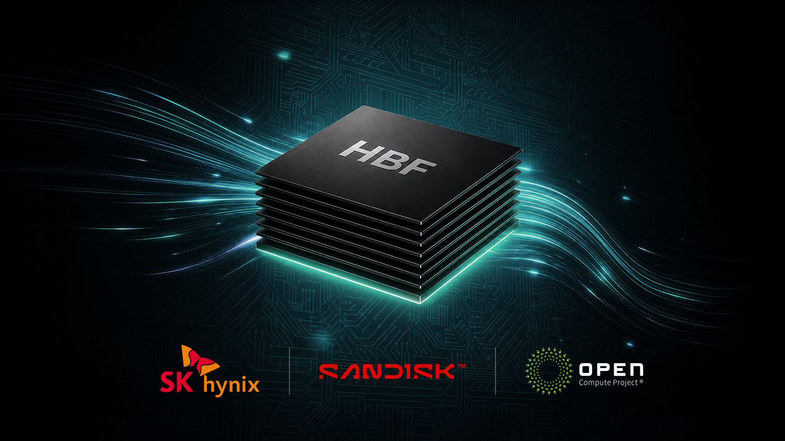
High Bandwidth Flash (HBF) is a new, open memory specification — jointly developed by Sandisk and SK hynix and published through the Open Compute Project (OCP) — for NAND-based chips that sit between HBM (High Bandwidth Memory) and ordinary SSD storage. The published spec describes stacks of up to 512GB that connect directly to CPUs, GPUs and AI accelerators over UCIe, at bandwidths from roughly 0.4TB/s to 3.0TB/s depending on the configuration. It is a standards milestone, not a product launch: no company has announced a shipping HBF chip, a price, or a specific release date.
The short version:
- What it is: A new memory tier — flash-based, not DRAM-based — meant to sit between HBM and SSD/NAND storage in AI systems.
- Who made it: Sandisk and SK hynix co-developed it; Google and Tenstorrent have joined the standardization consortium.
- Where it's published: As an open technical specification through the Open Compute Project, not as a proprietary product.
- Reported specs: Up to 512GB per stack (8-high or 16-high NAND die configurations), three bandwidth grades from about 0.4TB/s to 3.0TB/s, connected via UCIe.
- What's not confirmed: No commercial products, no pricing, and no firm consumer or enterprise launch date.
What Is High Bandwidth Flash (HBF)?
High Bandwidth Flash is a specification for packaging NAND flash memory — the same underlying technology used in SSDs and USB drives — into a stacked chiplet that behaves more like a high-speed memory module than a conventional storage drive. Instead of talking to a system over a storage protocol like NVMe, an HBF stack connects straight to a processor's package over a high-speed interconnect, the way HBM does today.
The idea, as described by Sandisk and SK hynix, is to fill a gap in the memory hierarchy. On one side sits HBM: extremely fast (multiple terabytes per second) but limited in capacity and expensive to scale, because it's built from stacked DRAM. On the other side sits SSD storage: enormous capacity and comparatively cheap, but far too slow and latency-heavy to feed a processor directly. HBF is pitched as a middle layer — slower than HBM, but dramatically faster than SSD, and with much higher capacity than HBM at a comparable cost, because it's built from NAND rather than DRAM.
Crucially, HBF is not meant to replace HBM. Every piece of coverage and both companies' own newsroom posts describe it as a companion tier that works alongside HBM in the same system — HBM handling the most latency-sensitive compute, HBF handling the much larger pool of "warm" data, such as large AI model weights or long-context key-value caches, that doesn't fit in HBM's limited capacity.
Who Announced HBF, and When
The HBF effort has unfolded in three public stages so far:
- August 2025: Sandisk and SK hynix announced a memorandum of understanding to collaborate on standardizing HBF, with Sandisk saying at the time that it was targeting first HBF memory samples in the second half of 2026 and samples of early AI-inference devices using HBF in early 2027.
- February 2026: The two companies formally kicked off an HBF standardization consortium at Sandisk's headquarters in Milpitas, California, launching a joint workstream under the Open Compute Project to turn the concept into a published technical specification.
- August 2026: Sandisk and SK hynix published the first official HBF technical specification through OCP, timed to the opening of the FMS (Future of Memory and Storage) 2026 conference in Santa Clara. Google and Tenstorrent were named as having joined the consortium during the standardization process, as detailed in Sandisk's own announcement.
That last step — the actual publication of a technical specification — is what this article is about. It's the point where HBF moved from a roadmap slide to a document other companies can read and build chips against.
How HBF Differs From HBM and SSD/NAND Storage
It helps to compare HBF against the two memory types it sits between. HBM is stacked DRAM, wired directly next to a processor die for maximum bandwidth and minimum latency, but DRAM is expensive to manufacture in large quantities and HBM stacks top out at a relatively modest capacity per stack. Conventional SSD storage uses NAND flash, which is dramatically cheaper per gigabyte and scales to huge capacities, but it talks to the rest of the system over a storage interface (like PCIe-based NVMe), with latency and bandwidth nowhere close to what a processor needs for active computation.
HBF tries to borrow the best of both: NAND's cost and capacity advantages, packaged and wired the way HBM is, so it can serve as active working memory rather than cold storage.
| Attribute | HBM (HBM4) | High Bandwidth Flash (HBF) | SSD / Plain NAND |
|---|---|---|---|
| Memory type | Stacked DRAM | Stacked NAND flash | NAND flash |
| Typical capacity | Up to ~64GB per stack | Up to 512GB per stack (8-high or 16-high) | Multiple terabytes per drive |
| Bandwidth per stack | Up to ~2TB/s (JEDEC JESD270-4 limit) | ~0.4TB/s to 3.0TB/s (3 grades) | Gigabytes per second (protocol-limited) |
| Connection to processor | Direct package interconnect | UCIe (direct package interconnect) | PCIe / NVMe storage link |
| Primary role | Fastest, latency-critical working memory | Large-capacity "warm" memory tier alongside HBM | Cold storage / bulk data |
| Status (Oct 2026) | Shipping standard, in production products | Open spec published; no commercial products yet | Widely available |
The bandwidth comparison is worth dwelling on. HBM4, the current JEDEC-standardized generation of HBM (JESD270-4, finalized in 2025), tops out at around 2TB/s of host-interface bandwidth per stack under its official specification. The top published HBF grade — 3.0TB/s — is reported to exceed that per-stack ceiling, even though HBF is built from slower NAND rather than DRAM. That's possible because HBF's bandwidth figure describes the width and speed of its UCIe host interface, not the raw read/write speed of the NAND cells themselves — the interface can be built wide and fast even when the underlying flash media is comparatively slow, which is also why HBF's real-world latency for AI workloads is expected to remain well above HBM's.
The Published Specs: Capacity, Bandwidth, and UCIe
According to the technical specification and both companies' newsroom coverage, HBF defines:
- Capacity: Up to 512GB per stack, built from two die-stack configurations — 8-high and 16-high NAND die stacks.
- Bandwidth: Three performance grades, reportedly spanning roughly 0.4TB/s at the low end up to 3.0TB/s at the high end.
- Interconnect: UCIe (Universal Chiplet Interconnect Express), the same open chiplet interconnect standard increasingly used to link separate dies within a single processor package — meaning HBF stacks are designed to sit on-package next to a GPU, CPU or AI accelerator die, not on a separate expansion card.
- Specification scope: The document reportedly covers the host (xPU-to-HBF) interface, electrical characteristics, baseline performance expectations, reliability and packaging guidelines for the die stack, and a software guide for read/write operations.
Because UCIe is an open, multi-vendor interconnect rather than a proprietary link tied to one company's chips, the pitch is that any accelerator maker could, in principle, design a processor package that talks to HBF stacks from any compliant memory vendor — the same multi-sourcing model that has long applied to standard DRAM and, more recently, to HBM itself.
Why HBF Matters for AI Inference
The driving problem HBF is aimed at is specific to AI inference at scale: modern large language models and other generative AI systems can have memory footprints — model weights plus the "key-value cache" that grows with every token of context — that vastly exceed what a GPU's onboard HBM can hold. Today, when that happens, systems either spread the model across many GPUs (expensive, and often underutilizing each chip's compute for the sake of its memory) or spill data out to much slower storage over a network or PCIe link, hurting throughput and latency.
HBF's pitch is that a single accelerator package could carry a much larger, cheaper, flash-based memory pool directly alongside its HBM, letting it serve more of a model — or serve more concurrent users and longer context windows — without multiplying the number of expensive GPUs needed. Sandisk has publicly framed this around "token economics": the idea that a flash-based memory tier that's slower than HBM but dramatically cheaper per gigabyte can lower the cost of serving each unit of AI output at scale, even if it can't match HBM's raw speed.
This also connects to a broader memory-market story that's been building all year: DRAM and HBM capacity has been tight and prices volatile as AI buildouts compete with everyday PC and server demand — a dynamic covered in Pandromeda's look at why RAM and DDR5 prices have climbed in 2026. A flash-based alternative that offloads some memory demand away from DRAM-based HBM is, at least in theory, one way to relieve part of that pressure for AI-specific workloads, even if it does nothing for consumer DDR5 pricing directly.
Could HBF Ever Reach Gaming GPUs?
The honest answer right now is: not announced, and not soon. Everything Sandisk, SK hynix and the OCP specification itself describe is scoped to AI accelerators and inference systems — the language used throughout is "xPU" (general-purpose, GPU, or custom AI processor) in a data-center context, not consumer graphics cards.
That said, the idea of flash-based memory eventually reaching enthusiast GPUs isn't invented by outside speculation alone — Sandisk itself has previously floated the concept publicly as part of its longer-term HBF vision, suggesting that future, higher-capacity revisions of the underlying technology could theoretically let a GPU carry several terabytes of total memory rather than the tens of gigabytes typical of today's high-end cards. That is a forward-looking concept illustration, not a product roadmap, and it comes with real technical caveats: NAND flash has finite write endurance, meaningfully higher latency than DRAM, and reportedly needs data managed in larger chunks than a GPU's memory controller is built for today — all problems a company would need to solve in software and silicon before any consumer GPU could use it. If you're deciding whether to buy a graphics card now or wait, HBF is not a reason to pause — nothing about it is close enough to consumer hardware to factor into a 2026 purchase.
Who's Behind the HBF Standard
Sandisk (the standalone NAND and storage company spun out of Western Digital) and SK hynix — one of the world's largest memory manufacturers and a dominant HBM supplier — are the specification's primary authors and the companies that have published the bulk of the public material about it. Both bring decades of NAND and (in SK hynix's case) HBM stacking and packaging experience to the effort.
Google and Tenstorrent have been named as having joined the HBF consortium during the standardization process — Google as a major AI infrastructure operator with an obvious interest in cheaper, denser AI memory, and Tenstorrent as an AI accelerator design company. Because the specification is published through the Open Compute Project rather than held as a private standard between two companies, other memory makers, accelerator designers and hyperscalers are free to review it and, in principle, build compatible products or join the workstream — which is the entire point of standardizing it through OCP rather than shipping it as a proprietary Sandisk/SK hynix product.
It's also worth noting, for context on who these companies are to Pandromeda's readers, that SK hynix (along with Samsung and Micron) is currently named in an ongoing DRAM price-fixing lawsuit — a separate legal matter unrelated to the HBF standardization effort, but relevant background on the same company.
What's Confirmed vs. What's Still Unknown
Pandromeda's style is to separate what's actually been announced from what's being inferred or projected. Here's that breakdown for HBF, as of this article's publication.
Confirmed, from the companies and the published specification:
- HBF is a real, jointly developed, open technical specification, published through the Open Compute Project in August 2026.
- It defines stacks up to 512GB, in 8-high and 16-high NAND die configurations.
- It defines three bandwidth grades spanning roughly 0.4TB/s to 3.0TB/s, using UCIe as the host interconnect.
- Sandisk and SK hynix are the lead developers; Google and Tenstorrent have joined the standardization consortium.
- The effort has a multi-stage public history: an August 2025 MOU, a February 2026 consortium kickoff, and the August 2026 specification publication.
Not yet announced or confirmed:
- No commercial HBF product from any manufacturer has been announced.
- No pricing — per-gigabyte or otherwise — has been published.
- No firm date for first commercial AI-inference systems using HBF; Sandisk has previously talked about sample timing (second half of 2026 for memory samples, early 2027 for early inference-device samples), but samples are not shipping products, and no company has committed to a retail or enterprise-availability date.
- No consumer or gaming GPU implementation has been announced, discussed as a near-term plan, or given any timeline by any company.
- Real-world performance, power consumption and reliability figures outside of the specification's own stated targets have not been independently measured, because no hardware is publicly available to test.
How HBF Fits Into the Broader Memory Market
HBF arrives at a moment when AI accelerator memory has become one of the tightest bottlenecks — and most expensive line items — in building AI infrastructure. HBM pricing and supply have been under strain as GPU makers compete for limited stacked-DRAM capacity, a squeeze that has also spilled over into conventional DRAM and DDR5 pricing for PCs, as Pandromeda has covered separately. A standardized, NAND-based alternative that multiple vendors can build to the same spec — rather than a single company's proprietary memory — is explicitly meant to avoid repeating that supply bottleneck: by publishing HBF openly through OCP instead of keeping it proprietary, Sandisk and SK hynix are inviting other NAND and packaging companies to eventually produce compatible parts, which, if it happens, would be good for competition and pricing in a way a single-vendor product would not be.
Whether that actually plays out depends entirely on uptake — a published specification is a necessary first step toward a competitive, multi-vendor memory tier, but it doesn't guarantee one. JEDEC-standardized memory types like DDR and HBM took years between initial specification and broad multi-vendor shipping products; there's no public reason yet to expect HBF to move dramatically faster, even though the underlying NAND manufacturing processes are already mature.
What's Next for HBF
The next milestones to watch, based on what's already been publicly stated, are the sample timelines Sandisk has previously described: HBF memory samples targeted for the second half of 2026, and samples of early AI-inference systems built around HBF targeted for early 2027. Neither of those is a retail or general-availability date, and neither has been reconfirmed with a specific date since the August 2026 specification was published.
Beyond that, the things actually worth watching are: whether any additional memory makers (beyond Sandisk and SK hynix) announce plans to build HBF-compliant parts now that the spec is public; whether any AI accelerator vendor announces a specific chip or system that uses HBF; and whether pricing or performance figures get published once real silicon exists to measure. Until then, HBF remains exactly what this article has described it as — a published, open, multi-vendor specification for a new flash-based memory tier, backed by two major memory companies and adopted in principle by at least two more, but with no shipping product, no price, and no confirmed launch date.
Frequently asked questions
Is High Bandwidth Flash (HBF) a real product you can buy?
Not yet. HBF is currently an open technical specification published by Sandisk and SK hynix through the Open Compute Project in August 2026. No company has announced a shipping HBF product, a price, or a specific launch date.
What is High Bandwidth Flash in simple terms?
It is NAND flash memory packaged and connected like high-speed memory rather than like a storage drive, designed to sit between HBM and SSD storage and give AI accelerators much larger memory pools than HBM alone can affordably provide.
How is HBF different from HBM?
HBM is built from stacked DRAM and is extremely fast but limited in capacity per stack. HBF is built from stacked NAND flash, offers far more capacity per stack (up to 512GB versus roughly 64GB for HBM4), but has higher latency and is meant to complement HBM, not replace it.
What bandwidth and capacity does the HBF spec define?
The published specification describes stacks of up to 512GB using 8-high or 16-high NAND die configurations, with three bandwidth grades ranging from roughly 0.4TB/s to 3.0TB/s, connected to processors over the UCIe interconnect.
Will HBF ever be used in gaming graphics cards?
Sandisk has floated the long-term idea of much larger GPU memory pools using flash-based memory, but every current announcement and the published spec itself are scoped to AI accelerators and data-center inference systems. No consumer GPU implementation has been announced or given a timeline.
Who is developing the HBF standard?
Sandisk and SK hynix are the lead developers and co-authors of the specification. Google and Tenstorrent have joined the standardization consortium under the Open Compute Project, and because it is an open spec, other memory and chip makers can build compatible products.
Sources
- SK hynix Newsroom: SK hynix Unveils First HBF Standard Specifications with Sandisk at FMS 2026news.skhynix.com
- SK hynix Newsroom: SK hynix and Sandisk Begin Global Standardization of Next-Generation Memory 'HBF'news.skhynix.com
- Sandisk Newsroom: Sandisk and SK hynix Advance Global Standardization of High Bandwidth Flashsandisk.com
- Sandisk Newsroom: Sandisk to Collaborate with SK hynix to Drive Standardization of High-Bandwidth Flash Memory Technologysandisk.com
- Open Compute Projectopencompute.org
- Wikipedia: High Bandwidth Memoryen.wikipedia.org
Mara Lindqvist edits the hardware desk. She covers graphics cards, processors, memory and storage, the foundries and chip designers behind them, and what the numbers on a spec sheet mean for people choosing a PC. Specifications in her stories come from manufacturer spec pages and datasheets.